
Outline
Welcome to the web site of Prof. Kazuto ARAKAWA Laboratory at Next-Generation Tatara Co-Creation Centre (NEXTA), Shimane University.
Crystalline lattice defects (point defects (vacancies and self-interstitial atoms), point-defect clusters, and dislocations, etc.) – local disorders of atomic arrangement - often govern macroscopic properties of various energy-related materials, such as nuclear-fission and fusion materials, boiler materials for thermal power plants, high-pressure hydrogen storage materials, bonding wires for LSI, and light-emitting devices, and general structural materials such as bridge materials. However, even for pure metals with comparatively simple structures, structures and behaviors of defects have been remaining to be clarified.
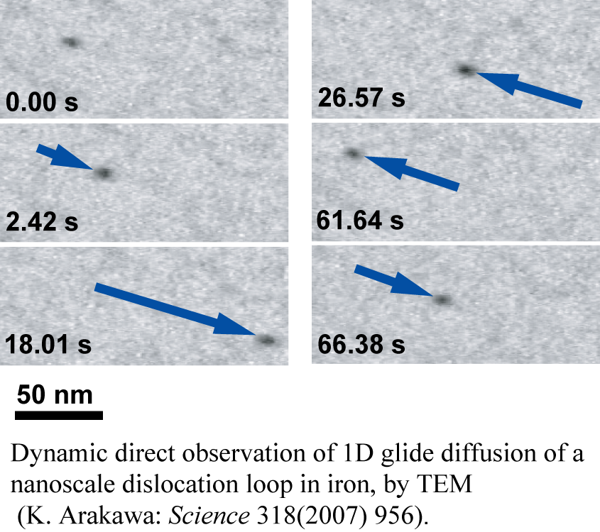 Transmission electron microscopy (TEM) is an extremely useful technique for observing structures and dynamic behaviors of local structures such as defects in real space. By direct TEM observations of behaviors of individual nanoscale defects in metals and semiconductors, we have uncovered important properties of them (K. Arakawa et al.: Nature Materials (2020), K. Arakawa et al.: Science (2007), K. Arakawa et al.: Physical Review Letters (2006), etc). Recently, we succeeded in extracting behaviors of ultra-fast moving single point defects (T. Amino, K. Arakawa et al.: Scientific Reports (2016)).
Our laboratory is driving researches on defects using TEM. Our goals are (1) establishment of the bases for prediction of accumulation processes of defects under defect-introduction environments and the consequential macroscopic-property variation, and (2) developments of new-functional materials based on the controls of defect behaviors, which we call “defect engineering.”